
RF PCB Design Guide for Defence Electronics
Stack-up, controlled impedance, grounding, EMC and environmental design: the PCB decisions that decide whether an RF or defence board works in the field.
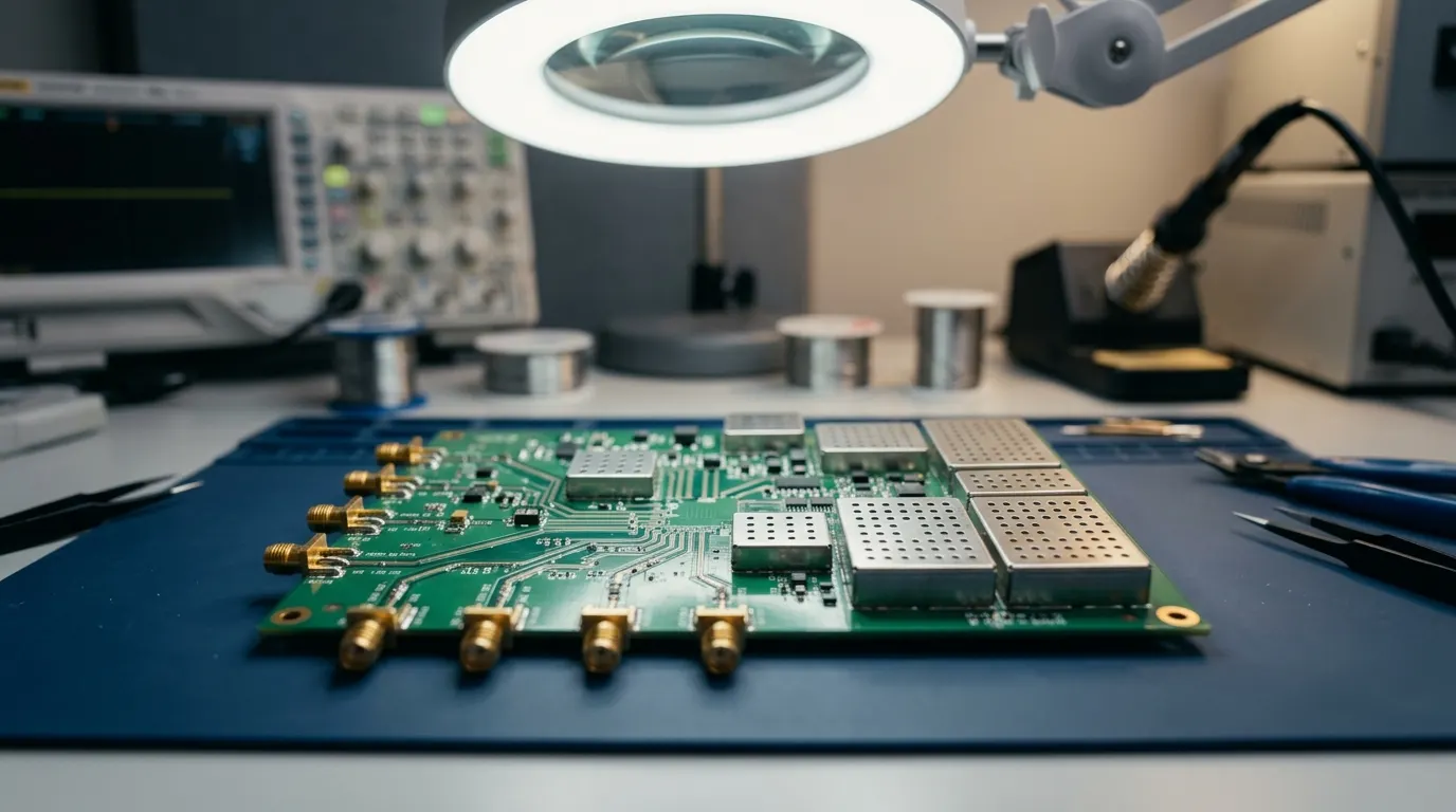
PCB design is where an electronic concept becomes hardware. For RF, navigation and military control electronics, the board is not just a carrier for components: the stack-up, trace geometry, grounding and layout determine signal integrity, noise, emissions and how the product survives heat, vibration and humidity. This guide covers the decisions that matter most when designing PCBs for defence and RF applications.
Start with the stack-up
The layer stack-up is the foundation of a multi-layer PCB. It sets the dielectric thickness between signal and reference planes, and therefore the impedance of every trace and the coupling between layers. A good RF stack-up places a solid ground plane directly under every RF layer, separates noisy digital and power layers from sensitive analogue ones, and keeps the build symmetrical so the board does not warp.
- RF layers adjacent to an uninterrupted ground plane
- Dedicated power planes with close-coupled ground for low impedance
- Low-loss laminate where frequency and trace length make loss significant
- Symmetrical build to control warpage during assembly
Controlled impedance and transmission lines
At RF frequencies a trace is a transmission line. Microstrip, stripline and grounded coplanar waveguide are the usual structures, and their width, spacing and dielectric height must be calculated for the target impedance — usually 50 Ω. Impedance mismatches cause reflections, ripple and loss, so controlled-impedance traces are specified on the fabrication drawing and verified by the board manufacturer.
Grounding, return paths and isolation
Most RF and EMC problems are really return-path problems. Every signal current returns through the reference plane directly beneath it; a split or slot in that plane forces the return current around it and creates a loop that radiates and picks up noise. Via fences along RF lines, stitching vias around the board edge and shielding cans over sensitive stages keep circuits isolated from each other.
EMC by design
Military equipment must coexist with radios, radars and power systems on the same platform. Designing for electromagnetic compatibility from the start is far cheaper than fixing emissions after testing:
- Keep fast switching loops — DC/DC converters, motor bridges — small and tightly coupled to ground
- Filter every cable entry; cables are the main antennas on most products
- Separate RF, digital and power sections physically and on the planes
- Choose edge rates and clock frequencies no faster than the design needs
Thermal and environmental design
Defence boards often run sealed, without airflow, across a wide temperature range. Thermal vias under power devices, copper pours as heat spreaders and a mechanical path to the enclosure keep junction temperatures under control. Conformal coating protects against humidity and contamination, and component selection, mounting and board thickness must suit the vibration and shock profile of the platform.
Design for manufacture and test
A design that cannot be built consistently is not finished. Pad geometries matched to the assembly process, test points on critical nets, clear fabrication notes for impedance and materials, and a review with the manufacturer before release reduce rework and keep performance repeatable from the first board to the last.
PCB design at Sağlamtek
Sağlamtek designs single-layer to multi-layer boards with RF-aware stack-ups, controlled impedance, grounding and EMC practice suited to defence environments — usually as part of an RF, antenna or control electronics product we develop for a specific platform. Because RF components, PCBs, antennas and mechanical integration are handled by the same engineering team in Ankara, interfaces between them are solved early rather than at integration. Our anti-jam GNSS systems, datalinks and motor drivers are built on this approach.

Written by
Sağlamtek Engineering Team
RF, antenna & navigation engineering · Ankara
Articles on this blog are written by the engineers who design, test and build Sağlamtek’s anti-jam GNSS, RF, antenna and radar products at our R&D Center and manufacturing facility in Ankara.